W&T Wetenschap & Technologie
Een plek om te discussiëren over wetenschappelijke onderwerpen, wetenschappelijke problemen, technologische projecten en grootse uitvindingen.


Updated: HP, Hynix plan to launch memristor memory in 2013
Peter Clarke
10/6/2011 11:27 AM EDT
SEVILLE, Spain – The 'memristor' two-terminal non-volatile memory technology, in development at Hewlett Packard Co. since 2008, is on track to be in the market and taking share from flash memory within 18 months, according to Stan Williams, senior fellow at HP Labs.
"We have a lot of big plans for it and we're working with Hynix Semiconductor to launch a replacement for flash in the summer of 2013 and also to address the solid-state drive market," Williams told the audience of the International Electronics Forum, being held here.
A spokesperson for HP added that there is no definitive memristor product roadmap as yet, but confirmed that "HP has a goal to see memristor products by the end of 2013."
Williams said that the memristor metrics being achieved, in terms of energy to change a bit, read, write time, retention and endurance, were so compelling that flash replacement was effectively a done deal. "So in 2014/2015 we'll be going after DRAM and after that the SRAM market," Williams said indicating his confidence that the memristor would quickly become a universal memory.
Williams declined to discuss in detail the process technology, memory capacity or memory-effect material that Hewlett Packard and Hynix are working with. "We're running hundreds of wafers through a Hynix full-size fab. We're very happy with it." But Williams did disclose that the first commercial memory would be a multi-layer device.
When challenged over the cost of the technology, which would be the barrier to competing against the high-volume flash memory market, Williams said: "On a price per bit basis we could be an order of magnitude lower cost once you get the NRE [non-recurring expense] out of the way."
The memristor, named after the combination of memory and resistor, was originally a theoretical two-terminal device for which the electrical behavior was derived by Leon Chua in 1971. However, in 2008 researchers from HP published a paper in Nature that tied the hysterical I-V characteristics of two-terminal titanium oxide devices to the memristor prediction of Chua. "What we found is that moving a few atoms a fraction of a nanometer can change the resistance by three orders of magnitude," said Webb. "In fact many nanodevices have inherent memresistive behavior," he said.
HP has amassed some 500 patents around the memristor over the last three years. He also acknowledged that phase-change memory (PCM), Resistive RAM (RRAM) and other two-terminal memory devices are all memristor-type devices. Williams acknowledged that many other companies are working on metal-oxide resistive RAMs. He said that Samsung now has a bigger research team working on the technology than does HP.
Williams touted the cross-point nature of the memristor memory switch or resistive RAM device as a memory capacity advantage over flash memory. "Whatever the best in flash memory is, we'll be able to double that."
Implication logic and the synapse
Williams compared HP's resistive RAM technology against flash and claimed to meet or exceed the performance of flash memory in all categories. Read times are less than 10 nanoseconds and write/erase times are about 0.1-ns. HP is still accumulating endurance cycle data at 10^12 cycles and the retention times are measured in years, he said.
One of the best things about the memristor memory is that it is a simple structure made using materials that are already common in the world's wafer fabs making CMOS-compatible devices relatively straight forward, he said.
This creates the prospect of adding dense non-volatile memory as an extra layer on top of logic circuitry. "We could offer 2-Gbytes of memory per core on the processor chip. Putting non-volatile memory on top of the logic chip will buy us twenty years of Moore's Law, said Williams.
Further out Williams said the memristor could be used for computation under a scheme called "implication logic" in a fraction of the area taken up in CMOS by Boolean logic. In addition a memristor device is a good analog of the synapse in brain function.
In conclusion Williams stressed that HP would not be getting into the semiconductor components business but would seek to commercialize and then license the technology to all comers
HP-Hynix-to-launch-memristor-memory-2013
Geld maakt meer kapot dan je lief is.
Het zijn sterke ruggen die vrijheid en weelde kunnen dragen
Het zijn sterke ruggen die vrijheid en weelde kunnen dragen

HP moves to revolutionize computingquote:HP moves to revolutionize computing
HP has worked up quite a reputation for being the king of drama over the last several years. However, this week the company shifted the drama where it belongs: with the products.
Yes, HP announced an ARM based server platform targeted at Cloud applications that promises to significantly reduce server costs for companies like Amazon, Google, Facebook and other entities who live off of the web.
Genre classics resurrected as graphic novelsYet, this is just the beginning of a much bigger revolution.
In a session after the announcement, HP Labs talked about the new as the first step to replace processor architectures, networking, and storage as we know it with a fabric based on their unique Memristor technology which is apparently close to initial test fabrication.
This would suggest HP is actually on the cusp of a revolution similar to the transistor. If properly executed, the new paradigm could put the company at the heart of an intense technology storm.
The Problem with Current Architectures
Remember, whether we are talking PCs or servers, the base architecture goes back decades to before there was a web or high speed networks. Repositories were, back in the days of yore, measured in megabytes. Now they are gauged in terabytes, with bottlenecks moving from slow processors, to slow memory, latency and crawling networks. As such, most forms of storage and traditional copper networking has become increasingly inadequate and will likely hit a wall in a few short years.
Add these limitations to the cloud, the massive movement of data to the most optimized resource, and virtualization. What do you get? The potential for the mother of all performance killers - the current server and storage architecture.
Memristors + Tiny Cheap Cores
But what if you could break the storage, networking, and processor elements into tiny parts that could be reassigned and grouped in close proximity on demand?
Well, Memristors represent the best aspects of both magnetic media (they are non-volatile) and flash (they are fast to read and write, consume little power, and are solid state). So, what if you took these storage elements and put them in groups in close proximity, perhaps on the same boards, as ARM processors?
You’d then have ultrafast high-capacity storage in extreme proximity to power efficient cores. Meaning, half Memristor-powered racks would likely be equivalent to several racks of more traditional products. In addition, the close proximity, coupled with the high on-board speed and optical fiber connections between the boards, should result in not only a sharp performance increase but also facilitate massive power savings.
While the end products likely would initially look a lot like existing server blades or rack mounted servers, they could be built in almost any configuration; as while the circuit density is high, the thermal requirements are actually comparatively low. Since proximity will be the major problem - imagine servers that look more like balls or cubes than they do today at some future point to minimize the distance between components that may need to dynamically share loads.
In short, HP opened up a can of whoop-ass on the technology market and we really don’t see that very often.
Wrapping Up: Personal Technology?
Smartphones and tablets kicked off the trend toward very low cost cores and eventually, what appears to be an aggressively redesigned computing architecture. However, many of these changes can be applied to future generations of PCs, tablets and smartphones - providing ever higher performance at ever lower battery life.
Just try and think of future devices that will revolutionize the market by making current-gen iPads and iPhones look fat, slow, and power hungry. Of course, irrespective of whether or not this actually happens, the good news is that HP is back to providing product drama, something which is long overdue. The Meg Whitman HP is certainly looking better and better all the time.
Geld maakt meer kapot dan je lief is.
Het zijn sterke ruggen die vrijheid en weelde kunnen dragen
Het zijn sterke ruggen die vrijheid en weelde kunnen dragen
quote:We report sub-nanosecond switching of a metal–oxide–metal memristor utilizing a broadband 20 GHz experimental setup developed to observe fast switching dynamics. Set and reset operations were successfully performed in the tantalum oxide memristor using pulses with durations of 105 and 120 ps, respectively. Reproducibility of the sub-nanosecond switching was also confirmed as the device switched over consecutive cycles.
iopsciencequote:In this work we demonstrated a platform for conducting
broadband dynamical studies of impedance mismatched
memristors. Tantalum oxide junctions were fabricated on
coplanar waveguide structures and reproducible resistance
switching of the order of 100 ps was shown. The measured
switching speed of this nonvolatile memory element is
comparable to or faster than mainstream volatile memories
such as DRAM and SRAM, and four orders of magnitude
faster than mainstream nonvolatile Flash. Additionally, the
result presented here opens new possibilities for the use of
memristors in high-speed high-frequency circuit applications.
......
The observed switching speed in this experiment was
limited by the pulse generator and not by the memristive device
itself nor by the transmission line structure. As a consequence,
one can envision that faster switching speeds in the double
digit picosecond range might be obtained by employing a faster
pulse generator as well as a compatible sample area in order to
minimize the parasitic effects associated with the memristor’s
parasitic capacitance.
Men heeft zelfs al ca 100 picoseconden schakeltijden gehaald met tantalium substraat memristor.
En het kan nog sneller want de testopstelling had erg veel last van parasitaire capaciteit en door die te reduceren zijn schakeltijden van enkele tientallen picoseconden haalbaar.
We hebben het dan over frequenties van ca 100 Ghz
Geld maakt meer kapot dan je lief is.
Het zijn sterke ruggen die vrijheid en weelde kunnen dragen
Het zijn sterke ruggen die vrijheid en weelde kunnen dragen
Klinkt interessant 
This might be a surprise but it's true
That I'm not like you and I don't want your advice
Or your praise or to move in the ways you do
And I never will
That I'm not like you and I don't want your advice
Or your praise or to move in the ways you do
And I never will
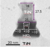
Bronquote:During IDEM, which is held in Washington, D.C. this week, the European research institute IMEC has shown the first 10nm RRAM cell. RRAM is often also referred to as a memristor.
The area of the cell is 100nm² and is based on hafnium/hafnium-oxide as the switching material. This material is placed between conventional contacts in a cross bar array. The contacts are made of titanium-nitride.
Cross section of IMEC 10nm RRAM cell. Copyright IMEC.
The cell has demonstrated an endurance of more than 1 billion reads/writes and switches in about 1ns. IMEC has extrapolated the data retention period to 10 years at 100 degrees C. Excellent life-span next to a hot GPU.
If manufacturing hurdles can be overcome, then this cell clearly demonstrates that RRAM will be superior to both NAND flash as well as conventional DRAM.
In order to use its potential fully then programmers will start to think of different ways to write programs since memory and storage over time could merge to one large linear space.
Hafnium als memristor-substraat is dus ook geschikt. Hafnium wordt sinds kort gebruikt als HKMG omdat hafnium-oxide een betere isolator is dan het gebruikelijke silicium-oxide. Bij de nanostucturen die men nu gebruikt kan men daarmee de aanzienlijke lekstromen reduceren. De halfgeleider industrie is dus als bekent met het toepassen van Hafnium in IC´s. Dit maakt een snelle lab to market introductie mogelijk zoals ook met het titanium wat HP gebruikt in hun memristors. Hafnium is echter veel kostbaarder dan titanium.
Geld maakt meer kapot dan je lief is.
Het zijn sterke ruggen die vrijheid en weelde kunnen dragen
Het zijn sterke ruggen die vrijheid en weelde kunnen dragen
Cool! Ik heb memristors altijd al interessant gevonden ivm de "continue" opslag eigenschap die erg lijkt op die van een synaps in de menselijke hersens. (Natuurlijk is dit maar een klein klein onderdeel van de mechanismen daar..)quote:Op donderdag 15 december 2011 23:07 schreef Digi2 het volgende:
[..]
Bron
[ afbeelding ]
Hafnium als memristor-substraat is dus ook geschikt. Hafnium wordt sinds kort gebruikt als HKMG omdat hafnium-oxide een betere isolator is dan het gebruikelijke silicium-oxide. Bij de nanostucturen die men nu gebruikt kan men daarmee de aanzienlijke lekstromen reduceren. De halfgeleider industrie is dus als bekent met het toepassen van Hafnium in IC´s. Dit maakt een snelle lab to market introductie mogelijk zoals ook met het titanium wat HP gebruikt in hun memristors. Hafnium is echter veel kostbaarder dan titanium.
Bronquote:Elpida Announces 64Mb ReRAM, Sees 8Gb Product in 2013
Jan 26, 2012 12:03 Jyunichi Oshita, Nikkei Electronics
Elpida Memory had a press conference Jan 24, 2012, and Takao Adachi, who is responsible for the development of the new memory, explained about the latest technology.
The new ReRAM. Each of its four areas is a 64-Mbit memory array.
Elpida Memory Inc developed ReRAM (resistive random-access memory), which is expected to be one of the next-generation nonvolatile memories.
The company prototyped the ReRAM by using 50nm process technology to form 64-Mbit cell arrays and confirmed operation of all bits. It has already started making efforts towards commercialization of the ReRAM.
"We want to launch an 8-Gbit product made by using 30nm process technology (as the first product) in 2013," said Takao Adachi, director of Elpida. "We will be ready for full-scale volume production in 2014."
Elpida plans to target the ReRAM at mobile machines such as smartphones, tablet computers and notebook computers. It expects that the ReRAM will be used as cache memory to fill a performance gap between DRAM and NAND flash memory in those machines.
"We hope that it will eventually be a memory that can replace DRAM because mobile machine makers want to reduce the amount of DRAM (which consumes a large amount of power) as much as possible and replace it with nonvolatile memory," Adachi said.
At this point, however, many of its customers that develop video-related stationary machines and want to enhance the speed of SSD are showing interest in the ReRAM, he said.
The new ReRAM is a 1T-1R-type ReRAM developed by using variable resistance elements based on hafnium (Hf) oxide. Its data reading speed is 20ns or faster, and it can be rewritten one million times or more. Elpida plans to completely clarify the mechanism of its operation and reduce the variation in the operation of memory elements in the aim of increasing its capacity to higher than 1 Gbit.
Though the ReRAM was prototyped by using 6F2 cells this time, Elpida intends to use 4F2 cells for volume production of the memory and reduce cell area. It can be mass-produced in production lines for DRAMs. For volume production, the company aims to achieve a bit cost 30% lower than that of DRAM.
Elpida has already decided to develop only ReRAM as its next-generation nonvolatile memory and is not developing MRAM (magnetic random access memory) or PRAM (phase-change random access memory).
The ReRAM was developed in collaboration with Sharp Corp, Japan's National Institute of Advanced Industrial Science and Technology (AIST) and the University of Tokyo in a project sponsored by New Energy and Industrial Technology Development Organization (NEDO) (See related article). The project was launched in 2010.
Tweakers
Dus na HP komt nu ook Elpida 2013/2014 met commercieel memristor geheugen op de markt.
Geld maakt meer kapot dan je lief is.
Het zijn sterke ruggen die vrijheid en weelde kunnen dragen
Het zijn sterke ruggen die vrijheid en weelde kunnen dragen

quote:
wow, als dit er komt dan kan ik toch zeggen tegen mijn vrienden dat ik erbij was toen het bedacht werd op FOK!
quote:Panasonic and TSMC Tip Resistive RAMs at ISSCC
Foundry looking for embedded memory solution
-----------------------
By Mark LaPedus, SemiMD senior editor
The emerging resistive RAM (ReRAM) market continues to heat up, as Panasonic and Taiwan Semiconductor Manufacturing Co. Ltd. (TSMC) will describe new breakthroughs in the arena.
At the International Solid-State Circuits Conference (ISSCC) in San Francisco on Wednesday (Feb. 22), TSMC will describe a ReRAM as part of the silicon foundry’s push in the embedded memory space. TSMC, along with National Tsing Hua University in Hsinchu, Taiwan, will disclose the development of a 0.5-Volt, 4-Mbit embedded ReRAM macro, based on a 65nm logic process.
At ISSCC, Panasonic will describe an 8-Mbit multi-layered cross-point ReRAM macro. The device has a 443-MB/second write throughput at 8.2nm pulse widths, which is twice as fast as competing efforts, according to Panasonic. Read access time is said to be 25ns.
Last year, Panasonic claimed to be sampling a 2-Mbit ReRAM, based on a tantalum and oxygen (TaOx) process. The 8-Mbit ReRAM uses the same technology, reportedly based on a 0.18-micron process.
Panasonic's ReRAM structure (Source: Company)
The ISSCC announcements follow what could be the hottest technology within the next-generation memory space. Elpida, Hynix, IMEC, Micron, Samsung, Sharp, Sony and others are working on ReRAM. ReRAM is “based on the electronic switching of a resistor element material between two stable (low/high) resistive states. The major strengths of ReRAM technology are its potential density and speed,” according to IMEC.
FRAM, MRAM, phase-change, ReRAM and others fall into the so-called universal memory category. Developers of these technologies claim their respective technologies can replace DRAM, NAND and NOR — or all three.
Most next-generation memory types have failed to live up to their promises. They are difficult to make and scale. But some claim the floating gate structure in flash is expected to hit the wall at 14nm, thereby fueling the need for a new memory type.
There are a range of emerging applications for next-generation memories. One of the possibilities is so-called storage-class memories. In this application, there is a need for a new and faster memory that sits between the processor and DRAM in a system to boost I/O performance. In theory, a storage-class memory would offload many of the functions in a power-hungry DRAM.
Block diagram of ReRAM from National Tsing Hua University and TSMC (Source: TSMC, National Tsing)
Embedded is another application. Many foundries offer embedded DRAM IP for system LSIs and other applications, but the technology could soon hit the scaling wall.
In embedded applications, “MRAM and ReRAM have the most promise,” said Fu-Lung Hsueh, a TSMC fellow and director of the Design Technology Division for the foundry giant, in a brief interview at ISSCC.
For some time, TSMC and Qualcomm Inc. have been developing an embedded memory based on MRAM technology. In the future, Qualcomm hopes to incorporate the MRAM IP within its cell-phone chip offerings.
ReRAM is another possibility for the embedded market. TSMC and National Tsing Hua University are developing a ReRAM solution. Hsueh said the device is still in the “prototyping” stage and the work is being conducted at the university level.
That device is said to enable short write times at low voltages. The 4-Mbit macro has four 1-Mbit sub-arrays, comprising of 2,048 columns and 512 rows, according to a paper from TSMC and National Tsing Hua. The entities developed a body-drain-driven current-mode sense amplifier (CSA) and small voltage headroom (VHR) for larger sensing margins. Using a new sensing scheme, the device is said to have a 45ns random read time, according to the paper.

chipdesignmagazine
zdnetquote:Ook Sandisk zet in op SSD-killer ReRAM
Geheugen van de toekomst
22 februari 2012 | Jan Custers
ZDNet.nl
Flashgeheugenfabrikant Sandisk zet een team van specialisten op de ontwikkeling van ReRAM-geheugen. Dat zou zowel het hedendaagse werk- als opslaggeheugen kunnen vervangen.
Sandisk plaatste vorige week een vacature op zijn website voor een verantwoordelijke van een dertigkoppig onderzoeksteam dat de productie van op memristors gebaseerd resistief RAM-geheugen (ReRAM) mogelijk moet maken. Het doet dat in samenwerking met partner Toshiba. Dat merkte Bright Side of News op.
Technologie evolueert snel
Vorige maand beweerde de Japanse geheugenfabrikant Elpida dat het samen met elektronicagigant Sharp een prototype van ReRAM-geheugen had ontwikkeld met dezelfde lees- en schrijfsnelheden als het DRAM-geheugen in hedendaagse computers.
Ook Panasonic, Sony, Micron, DSI en HP - in samenwerking met Hynix Seminconductor – investeren in de technologie. Die steunt op de revolutionaire ‘memristor’ die HP in 2008 ontwikkelde. Het eerste commerciële ReRAM-product wordt rond 2013 verwacht.
Snel en niet-vluchtig
ReRAM wordt naar voren geschoven als de opvolger van zowel het huidige systeem- als opslaggeheugen in computers. De technologie combineert de lees- en schrijfsnelheid van DRAM-geheugen met de niet-vluchtige aard van flashgeheugen. Dat betekent dat gegevens bewaard blijven als de spanning wegvalt. In theorie zal een computer met genoeg ReRAM-geheugen geen laadtijden meer kennen.
Jammer genoeg ligt Elpida ff uit de race, het bedrijf heeft faillisement moeten aanvragen.
De ex CEO van Sandisk denkt ook dat de memristor de nieuwe generatie geheugen gaat worden.
De kaarten lijken geschut, alle grote geheugenfabrikanten zijn nu met reram in de weer met aanzienlijke teams. Voor flashgeheugen liggen er aanzienlijke obstakels bij verdere structuurverkleining. De energie en gelden die trachten te overkomen ziet men blijkbaar beter besteed in een nieuw type geheugen met nog legio mogelijkheden tot structuurverkleining, substraat optimalisaties en 3D implementatie.
Geld maakt meer kapot dan je lief is.
Het zijn sterke ruggen die vrijheid en weelde kunnen dragen
Het zijn sterke ruggen die vrijheid en weelde kunnen dragen
De opvolgers van Reram tekenen zich trouwens ook al af.
1. Moleculair geheugen.
Slechts 1 molecuul wordt gebruikt als schakelaar. IBM en HP doen hier veel onderzoek naar.
Dit geheugen kent geen ¨slijtage/material deformation¨ zoals flash en memristor geheugen.
Het is een eenvoudige spin-off van Oled technologie, een opkomende miljardenmarkt.
2. Quantum geheugen. Ook hier heeft IBM enige doorbraken gemaakt. Dit lijkt op Dram in de zin dat er ¨gerefreshed¨ moet worden vanwege decoherentie. Door het koppelen van enkele qubits is echter een schier oneindig geheugen in bits/bytes te defineren.
Bepaalde vraagstukken laten zich met quantumcomputers oplossen die voor klassieke digitale computers zeer moeilijk zoniet onmogelijk zijn.
Geld maakt meer kapot dan je lief is.
Het zijn sterke ruggen die vrijheid en weelde kunnen dragen
Het zijn sterke ruggen die vrijheid en weelde kunnen dragen
Gizmoquote:Samsung realizes ReRAM's rewritability of one trillion times
Resistive Random Access Memory (ReRAM) technology has been making the news rounds throughout the electronic market since its inception back in 1997. Panasonic had led the way for commercial mass production as this next generation iteration of non-volatile memory types is being developed by a multitude of companies. But this time, Samsung has rather notched a level by contriving a performance enhancing technology, which boosts the ReRAM's rewritability capacity to a mind-boggling 1 trillion times!
Fundamentally, this new advanced technology utilizes asymmetric Ta2O5-x/TaO2-x bi-layer laminated film as the resistivity-varying material, instead of the conventional Ta2O5 film. The new material contributes to localized resistance switching. The reduction in switching current in turn allows for lesser power consumption, along with extreme cycling endurance of over 1 trillion.
The figures speak for themselves as this touted one trillion mark capability is about one million times more than that of the latest flash memory. Moreover, with switching times of only 10ns, the fascinating technology can be applied in cases of working-memory space.

Geld maakt meer kapot dan je lief is.
Het zijn sterke ruggen die vrijheid en weelde kunnen dragen
Het zijn sterke ruggen die vrijheid en weelde kunnen dragen

Het is een combinatie van geheugen en weerstandquote:Op donderdag 29 maart 2012 18:49 schreef Senor__Chang het volgende:
Kan iemand dit uitleggen voor de leek?
Trots lid van het 👿 Duivelse Viertal 👿
Een gedicht over Maanvis
Het ONZ / [KAMT] Kennis- en Adviescentrum Maanvis Topics , voor al je vragen over mijn topiques!
Een gedicht over Maanvis
Het ONZ / [KAMT] Kennis- en Adviescentrum Maanvis Topics , voor al je vragen over mijn topiques!
Dus computers worden nog sneller ofzo? En wat zouden we dan met die extra snelheid kunnen doen dat zo revolutionair is?

Als ik het goed heb begrepen is het lijstje voordelen van zo'n component (als het doorontwikkeld wordt):quote:
Dus computers worden nog sneller ofzo? En wat zouden we dan met die extra snelheid kunnen doen dat zo revolutionair is?
- Minder energieverbruik om data te schrijven/lezen
- Sneller data wegschrijven
- Minder defect-gevoelig (want minder losse componenten)
- Meer data per vierkante cm. Altijd fijn.
Health In Harmony is een non-profitorganisatie die regenwoudgemeenschappen helpt met gezondheidszorg en duurzame inkomens in ruil voor bosbescherming, en zo tegelijk klimaatverandering en armoede aanpakt. - https://www.healthinharmony.org/


Ik ga uit van sarcasme maar toch nog even dit.quote:Op vrijdag 30 maart 2012 01:42 schreef Senor__Chang het volgende:
Oh ok, maar niks revolutionairs dus?
Elk technologische paradigma heeft een bepaalde levensduur totdat iets zo ver uitontwikkeld is dat er geen rek meer in zit. Electronenbuizen werden vervangen door transistors die de jaren daarop ook weer kleiner en kleiner werden. Transistors liepen ook weer tegen limieten aan qua productiesnelheid en toen gingen we allemaal over op integrated circuits.
Paradigmaverschuivingen zijn een essentieel onderdeel van de gemiddelde 35% per jaar kosten afname, snelheid/capaciteitstoename. Dat fenomeen heet ook wel Moore's Law

Besef even dat de verticale schaal logaritmisch is.
Health In Harmony is een non-profitorganisatie die regenwoudgemeenschappen helpt met gezondheidszorg en duurzame inkomens in ruil voor bosbescherming, en zo tegelijk klimaatverandering en armoede aanpakt. - https://www.healthinharmony.org/
|
|